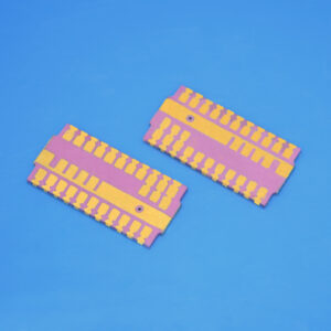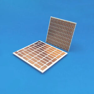



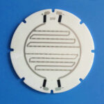
Services for Metallized Ceramic Substrate
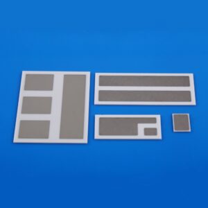
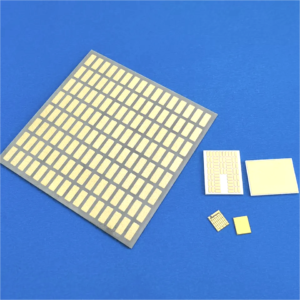
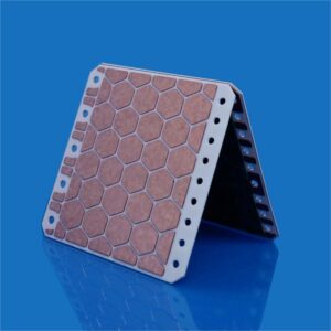
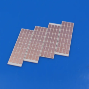
You can get rich supports in metallized ceramic substrate, our capabilities and services are as follows :
- Material:mainly Al2O3,AlN,Si3N4,BeO
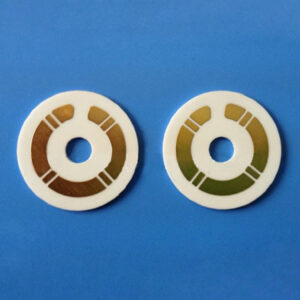
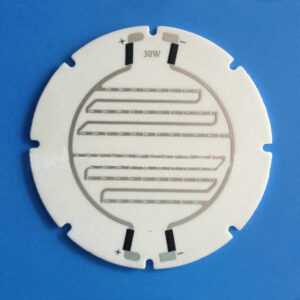
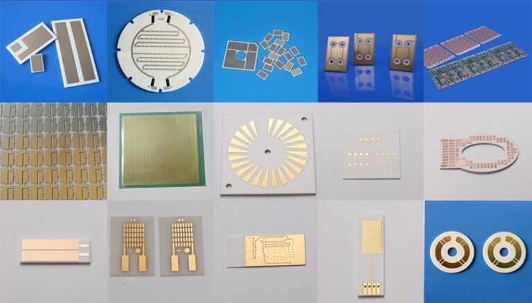
- Product type:Round, square, ring, triangle and other shapes
- Production process: mainly tape casting
- Surface finishing: grinding, laser cutting, metallization
- Processing accuracy: dimensional accuracy can be controlled to 0.03mm
Meet Customized Requirements
Standard thicknesses of substrates include: 0.25mm, 0.30mm, 0.50mm, 0.635mm, 0.80mm, 1.0mm, etc. If you have customized requirements for other thicknesses and shapes, we can also meet them.

Metallized Ceramic Substrate Classification
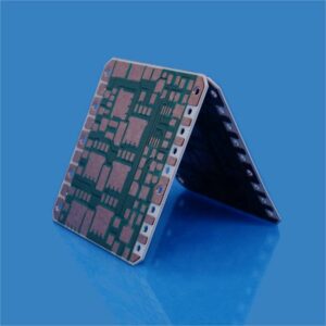
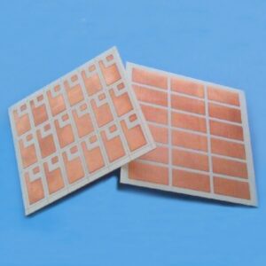
Metallized ceramic substrate includes bare ceramic substrate and metal line layer, bare ceramic substrate connects internal and external heat dissipation channels and mechanical support role, metal line layer makes circuit interconnections to complete the electrical function.
According to the package structure and application requirements, metallized ceramic substrates can be divided into flat ceramic substrates and three-dimensional ceramic substrates two categories, Jinghui ceramic currently only does processing of flat ceramic substrates, which are categorized as follows:
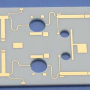
TFC
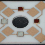
TPC

DBC
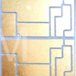
AMB
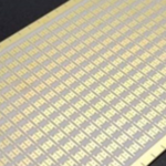
DPC
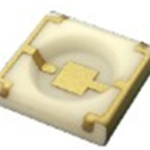
LAM
Main Characteristics of metallized Ceramic substrates
Semiconductor devices gradually to high-power, miniaturization, integration, multi-function and other directions, the performance of the package substrate also put forward higher requirements. Metallized ceramic substrates have some common performance requirements to be achieved.
high thermal conductivity
Current power semiconductor devices are thermoelectric separation package, most of the heat generated by the device through the package substrate spread out, good thermal conductivity of the substrate can make the chip from thermal damage.
Thermal Expansion Coefficient Matching
The chip is directly mounted on the package substrate, matching the coefficients of thermal expansion of the two will reduce the thermal stress of the chip and improve the reliability of the device.
Good heat resistance
Meet the demand of high temperature use of power devices, with good thermal stability.
Good insulation
Meeting device electrical interconnection and insulation needs,suitable for a wide range of high current and high voltage applications.
High mechanical strength
Meets the strength requirements of device processing, packaging and application.
The right price
Only when the price is right will mass production and wider application be possible.
Good chemical stability
Resistant to all kinds of strong acid and alkali corrosion, antioxidant, used in a variety of harsh environments.
Good surface flatness
Good curvature to ensure the consistency of heat dissipation and shrinkage of the sintered product.

