Advanced Electrical Ceramic Substrates
We are a professional manufacturer of ceramic substrates in China, with many years of production experience and unique technical advantages. Ceramic substrates are widely used in LED lighting, semiconductor, medical and other fields due to their excellent thermal, mechanical, chemical and dielectric properties.
We have complete production equipment and quality management system, and strictly follow the ISO9001 standard to ensure the quality and stability of our products. We continue to innovate and optimize product performance to provide customers with better services and products. Looking forward to cooperate with you.
Table of Contents for this Page
It is not easy to introduce all aspects of Ceramic Substrates, so we have prepared a lot of information on this page for you to delve into. To make sure you can find the information you want quickly, we have prepared this content directory that will jump to the corresponding location when you click on it.
the Typical Applications
As the carrier of circuits, ceramic substrates have been used in LED lighting, semiconductor devices, power electronics, communication equipment, aerospace, automotive electronics, military and other fields.

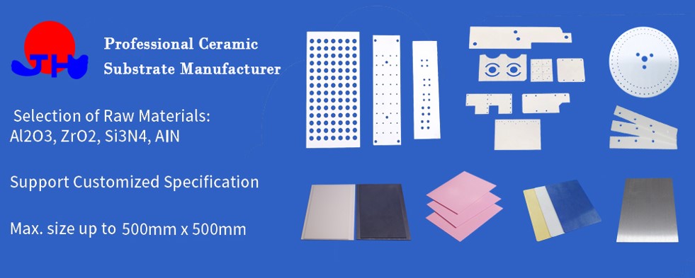
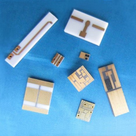
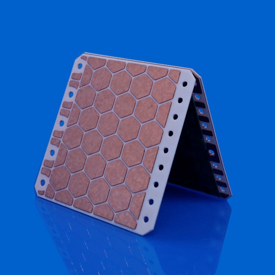
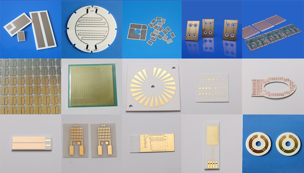
Hot Products Display
We classify Ceramic Substrates into 2 types:
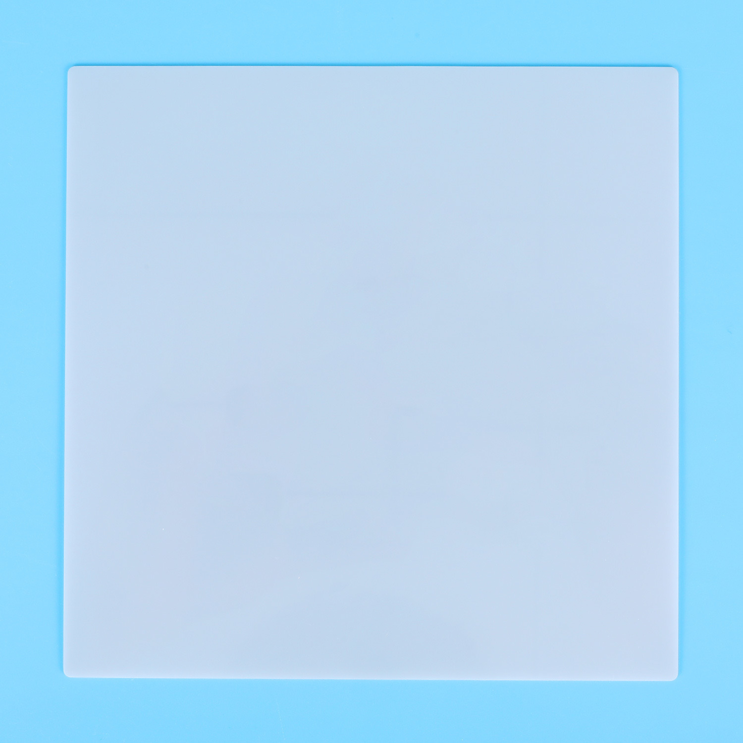
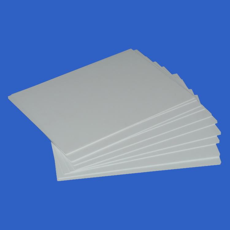
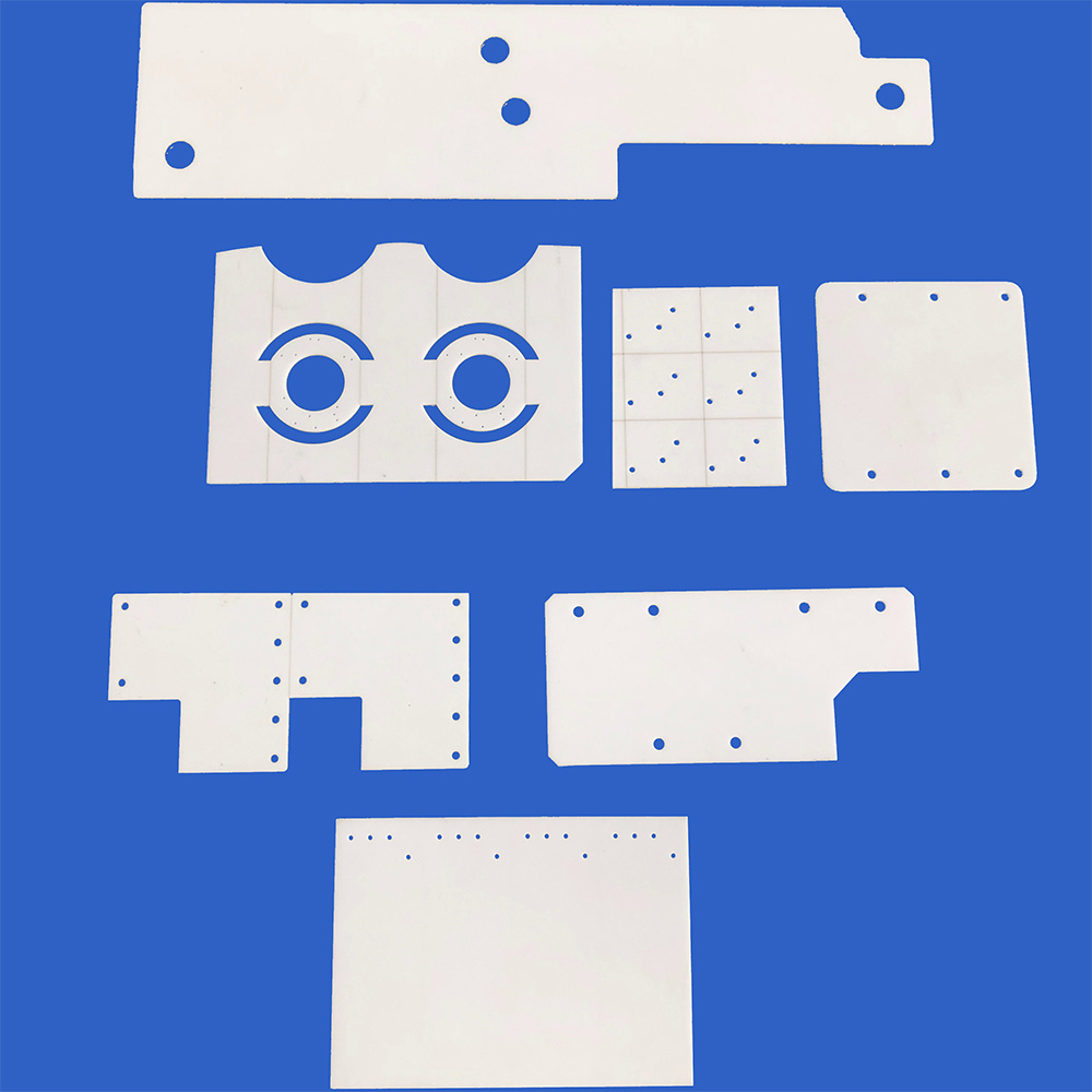
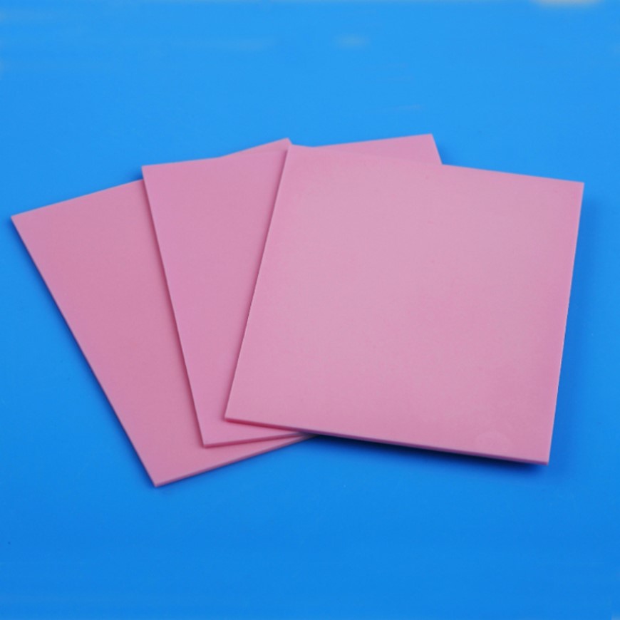
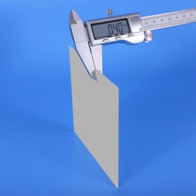
1) Bare Ceramic Substrates
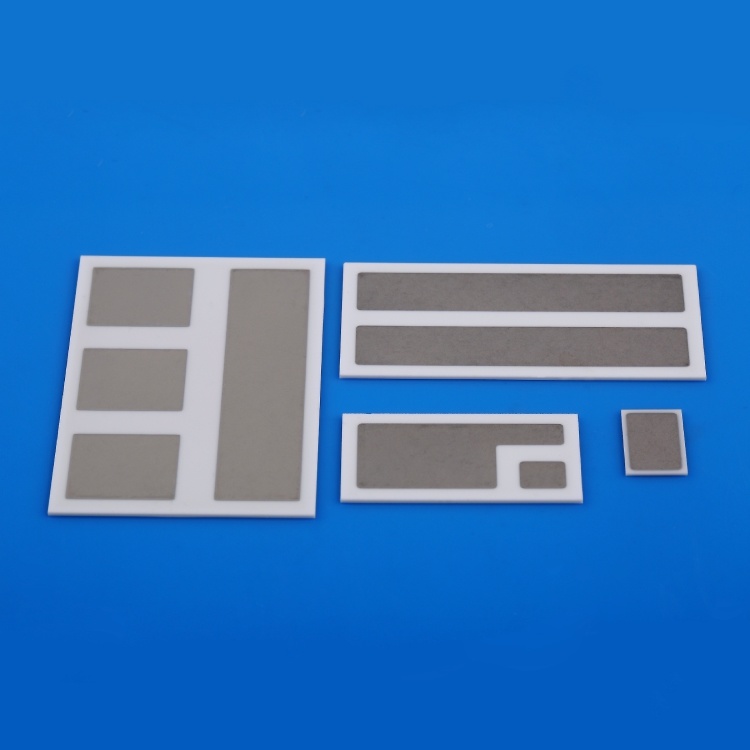
2) Metallized Ceramic Substrates
You can find the products you need from our classification.
Reference Cost Analysis
There are mainly the following 4 factors that affect your purchase cost, which need to be carefully considered before you place a purchase order.
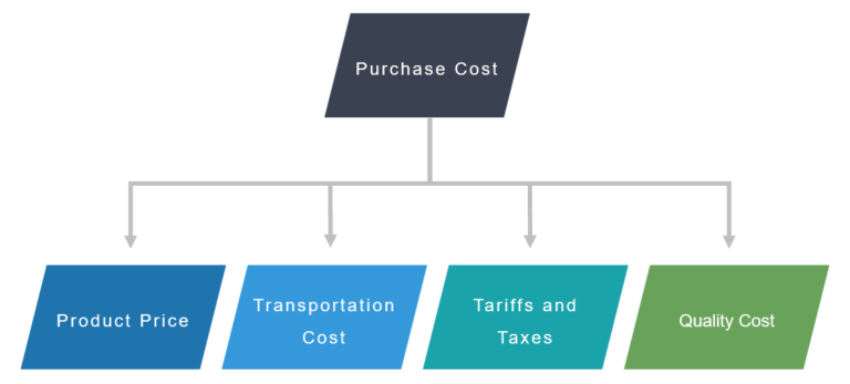
- Purchase Price: Main cost; Influencing factors: production process, raw material cost, order quantity and customization requirements.
- Transportation Cost: Choosing: express, air, sea, train or truck; Considering: weight & volume of goods, delivery deadlines, shipping costs, and shipping safety.
- Tariffs and Taxes: Relatively fixed cost; Related factors: customs code, national policies and agreements, the value of imported goods and types of imported goods.
- Quality Cost: Hidden costs; Including: returns, replacements, repairs, etc; Our quality is reliable, almost no quality problems.
Estimated Lead Time
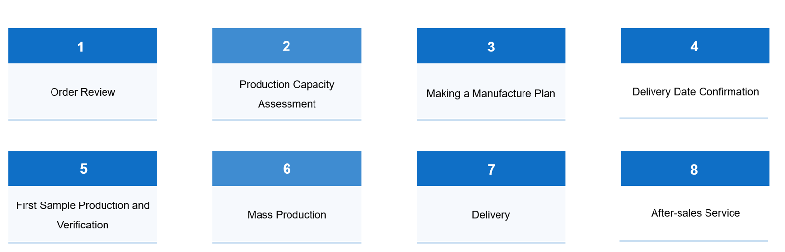
1. Product customization process
When we receive the customer’s order, we will process it according to the following standard process, mainly including 8 steps.
2. How long does it take from placing an order to receiving the goods?
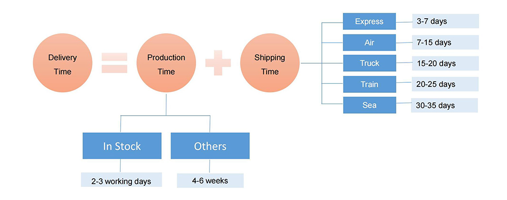
Want to know how to compress lead times?
If you are not satisfied with the delivery time or need us to expedite the shipment, please contact our sales in time to communicate.
the Basic Knowledge
1. About bare ceramic substrates
1.1 Bare ceramic substrates Introduction
Bare ceramic substrate, based on electronic ceramics, is a sheet material that forms a supporting base for membrane circuit components and external components. It has high temperature resistance, high electrical insulation performance, low dielectric constant and dielectric loss, high thermal conductivity, good chemical stability, similar thermal expansion coefficient to components, etc. It is often used as functional ceramic components in various hybrid integrated circuits, high-power modules, smart power semiconductors, automotive electronics, etc. The ceramic substrate is relatively brittle, and the substrate area is small and the cost is high. Generally, wiring, drilling, surface treatment, etc. are required.
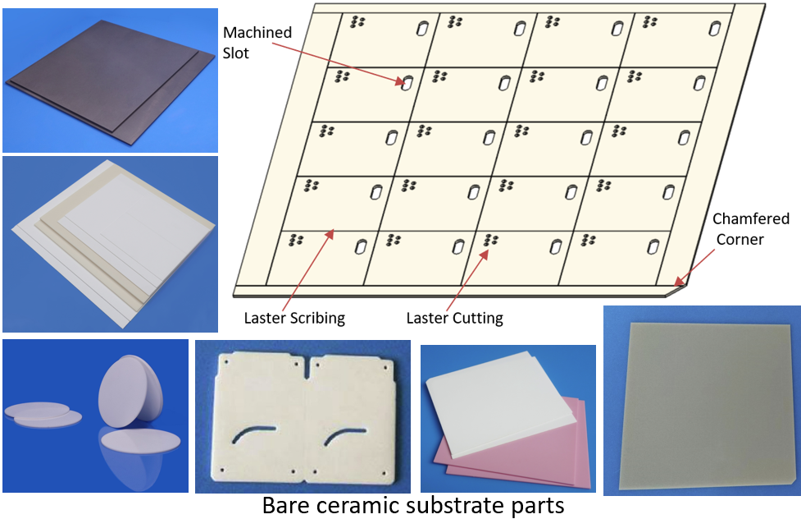
The mainstream ceramic substrates on the market include high-purity alumina ceramic substrate, aluminum nitride ceramic substrate, silicon nitride ceramic substrate and silicon carbide ceramic substrate, which have a wide range of applications and outstanding features. We specialize in tape casting process to produce ceramic substrates in various standard shapes, and can also provide customized shapes through secondary processing such as laser scribing, laser cutting, and precision machining. Standard thickness includes 0.25/0.30/0.38/0.50/0.635/0.80/1.0mm etc. Additionally, custom thicknesses can be achieved if desired.
1.2 Main characteristics of ceramic substrates
High Thermal Conductivity
Matchable CTE
Good Heat Resistance
Good Insulation
High Mechanical Strength
Reasonable Price
1.3 Material selection for bare ceramic substrates
1.3.1 Alumina
Alumina ceramics are the most widely used materials in ceramic substrates, but considering the thermal conductivity of its different purity products (96% Al2O3 to 99.6% Al2O3) from 20W/(m·K) to 31W/(m·K) , and the thermal expansion coefficient is 7.0×10⁻⁶/℃-8.0×10-6/℃ in the temperature range of 25℃-200℃. Therefore, alumina substrates are generally used in automotive electronics, semiconductor lighting, electrical equipment and other fields.
1.3.2 Aluminum nitride
The aluminum nitride material is off-white, belongs to the hexagonal crystal system, and is a wurtzite-type covalent bond compound with tetrahedron as the structural unit. This structure determines its excellent thermal, electrical and mechanical properties. The theoretical thermal conductivity of AlN ceramics can reach 320W/(m·K), the thermal conductivity of its commercial products is generally 180W/(m·K)-260W/(m·K), and the thermal expansion coefficient in the temperature range of 25°C-200°C is 4×10⁻⁶/℃ (basically matching with semiconductor chip materials such as Si and GaAs), and the dielectric constant is 8-10.
The thermal conductivity of aluminum nitride ceramics is 6-8 times that of alumina ceramics, but its thermal expansion coefficient is only 50%. In addition, it also has the advantages of high dielectric strength, low dielectric constant, and good corrosion resistance.
In addition to the high cost, the comprehensive performance of aluminum nitride ceramics is better than that of alumina ceramics. It is an ideal electronic packaging substrate material, especially suitable for fields with high thermal conductivity requirements.
1.3.3 Silicon nitride
Si3N4 has three crystal structures, which are α phase, β phase and γ phase (among which α and β phase are the most common forms), all of which are of hexagonal structure, and its powder and substrate are off-white. The Si3N4 ceramic substrate has an elastic modulus of 320GPa, a bending strength of 920MPa, a thermal expansion coefficient of only 3.2×10⁻⁶/°C, and a dielectric constant of 9.4. It has the advantages of high hardness, high strength, small thermal expansion coefficient, and high corrosion resistance. .
Among the existing ceramic materials that can be used as substrate materials, Si3N4 ceramics have high bending strength, good wear resistance, and are ceramic materials with the best comprehensive mechanical properties. At the same time, its thermal expansion coefficient is the smallest, so it is considered to be a potential substrate material for power device packaging. However, its preparation process is complicated, its cost is high, and its thermal conductivity is relatively low. It is mainly suitable for applications in fields with high strength requirements but low heat dissipation requirements.
2. Metallized ceramic substrates Introduction
Metallized ceramic substrate, also known as ceramic circuit board, includes a bare ceramic substrate and metal circuit layers.It is obtained by metallizing the surface of the bare ceramic substrate by technical means. According to the packaging structure and application requirements, ceramic substrates can be divided into two categories: planar ceramic substrates (TFC/TPC/DBC/DPC/AMB/LAM) and three-dimensional ceramic substrates (HTCC/LTCC/MSC/DAC/MPC/DMC).
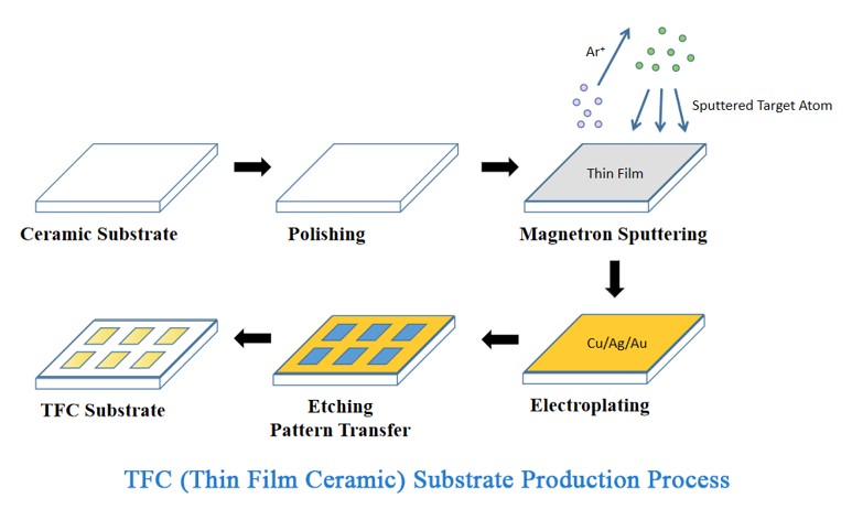
2.1 Thin film ceramic substrate (TFC)
Thin film ceramic substrate generally adopts sputtering process to directly deposit a metal layer on the surface of the ceramic substrate. If photolithography, development, etching and other processes are assisted, the metal layer can also be patterned into circuits. Due to the low sputtering coating deposition rate (generally less than 1 μm/h), the thickness of the metal layer on the TFC substrate is relatively small (generally less than 1 μm). It can prepare ceramic substrates with high graphic accuracy (line width/line spacing less than 10 μm), which are mainly used in the packaging of small current devices in the field of laser and optical communication.
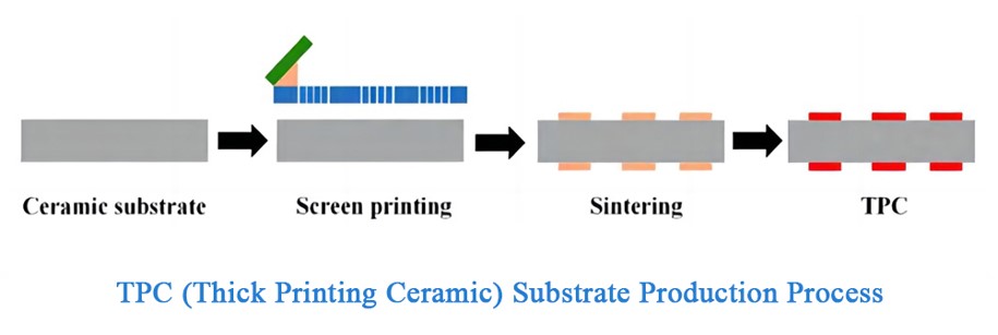
2.2 Thick printing ceramic substrate (TPC)
The metal paste is coated on the ceramic substrate by screen printing, and after drying, it is sintered at high temperature (the temperature is generally 850°C-900°C) to prepare the TPC substrate. Depending on the viscosity of the metal paste and the mesh size of the screen, the thickness of the prepared metal circuit layer is generally 10 μm-20 μm (increasing the thickness of the metal layer can be achieved by multiple screen printing).
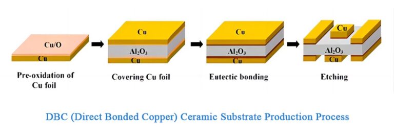
2.3 Direct bonded copper ceramic substrate (DBC)
DBC ceramic substrate preparation first introduces oxygen element between copper foil (Cu) and ceramic substrate (Al2O3 or AlN), and then forms CuO eutectic phase at 1065°C (metal copper melting point is 1083°C), and then react with the ceramic substrate and copper foil to form CuAO2 or Cu(AO2)2, realizing the eutectic bonding between copper foil and ceramics. Due to the good thermal conductivity of ceramics and copper, and the high eutectic bonding strength between copper foil and ceramics, DBC substrates have high thermal stability and have been widely used in insulated-gate bipolar transistors (IGBTs), laser diodes (LDs) ) and concentrating photovoltaic (CPV) and other devices in the package heat dissipation.
The thickness of the copper foil on the DBC substrate is relatively large (generally 100μm-600 μm), which can meet the application requirements of device packaging in extreme environments such as high temperature and high current. In order to reduce substrate stress and warpage, a ship adopts a sandwich structure of C1-A1O2C, and the upper and lower copper layers have the same thickness.
Although DBC substrates have many advantages in practical applications, the eutectic temperature and oxygen content must be strictly controlled during the preparation process, which requires high equipment and process control and high production costs.
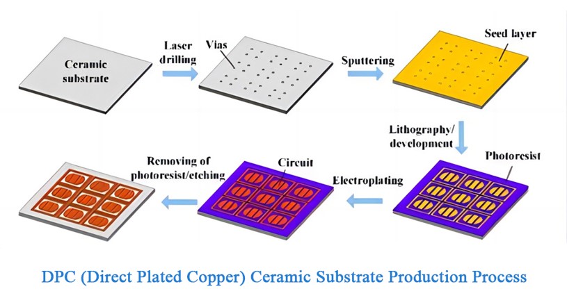
2.4 Direct plated copper ceramic substrate (DPC)
First, lasers are used to prepare through-holes on the ceramic substrate (the aperture is generally 60 μm-120 μm), and then ultrasonic cleaning is used to clean the ceramic substrate. Deposit a metal seed layer (Ti/Cu) on the surface of the ceramic substrate by magnetron sputtering technology, and then complete the circuit layer production by photolithography and development. Use electroplating to fill holes and thicken the metal circuit layer, and improve the solderability and oxidation resistance of the substrate through surface treatment. Finally, remove the dry film and etch the seed layer to complete the substrate preparation.
3. How to choose bare ceramic substrates and metallized ceramic substrates?
3.1 Material performance comparison
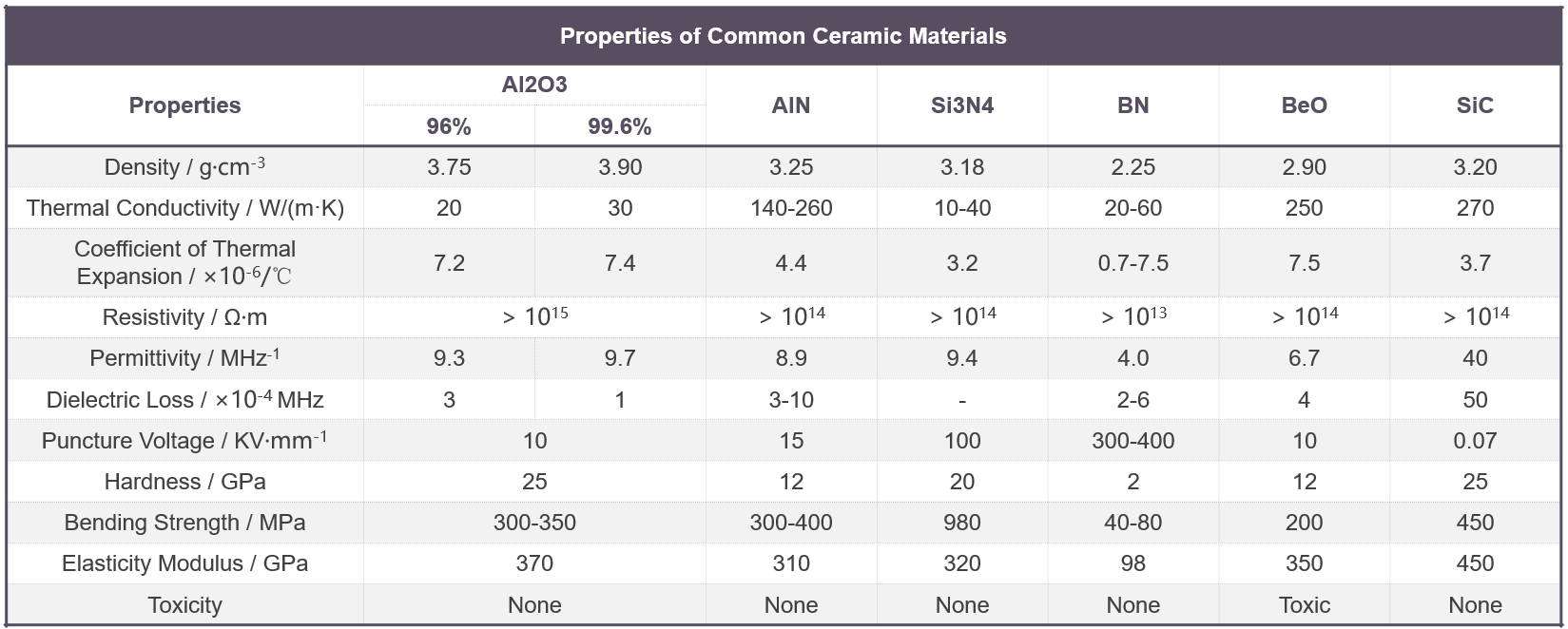
Commonly used ceramic substrate materials are alumina (Al2O3), aluminum nitride (AlN), silicon nitride (Si3N4), boron nitride (BN), beryllium oxide (BeO) and silicon carbide (SiC). The following is a comparison of their material properties.
3.2 Performance comparison of metallized ceramic substrates
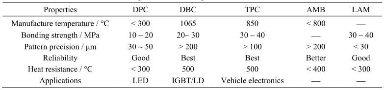
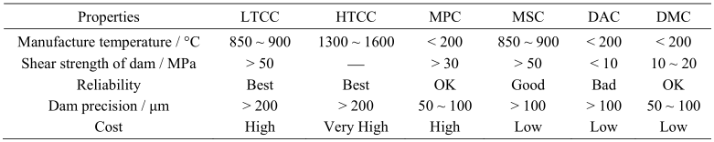
Among the planar ceramic substrates, the TFC substrate has high graphic precision, but the metal layer is thin, and is mainly used in the packaging of small current optoelectronic devices; the TPC substrate has good heat resistance, low cost, but poor circuit layer accuracy, and is mainly used in automotive sensors and other fields; DBC and AMB substrates have thicker circuit layers and better heat resistance, and are mainly used in high-power, large-temperature-changing IGBT packages; DPC substrates have the advantages of high graphic accuracy and vertical interconnection, and are mainly used in high-power LED packages; The LAM substrate meets the heat dissipation requirements of special-shaped ceramic structural parts in the aerospace field.
Among the three-dimensional ceramic substrates, HTCC/LTCC and MSC substrates are prepared by screen printing and high-temperature sintering processes, and the reliability of the cavity is high, but the accuracy of the metal circuit layer is poor; It has the advantages of high precision of the metal circuit layer and high bonding strength between the dam and the substrate, and is expected to play an important role in the fields of hermetic packaging, three-dimensional packaging and integration of power devices in the future.
The commonly used ceramic substrate materials in China are mainly Al2O3, AlN and Si3N4. Al2O3 ceramic substrate mainly adopts DBC process, AlN ceramic substrate mainly adopts DBC and AMB process, and Si3N4 ceramic substrate mostly adopts AMB process.The metallized ceramic substrate materials we produce mainly include alumina ceramics and aluminum nitride ceramics. Standard thickness covers 0.25/0.30/0.38/0.50/0.635/0.80/1.0mm. Mainly used in LED lighting, optical communication and information equipment, medical industry, automobile industry, environment and energy industry, etc.
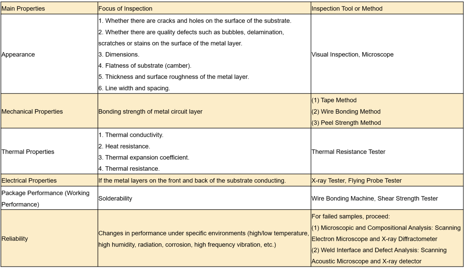
3.3 Inspection of ceramic substrates
In order to ensure that the quality of our ceramic substrates meets customer expectations, all of our products will undergo strict inspections before leaving the factory. Only products that pass the inspection will be shipped.
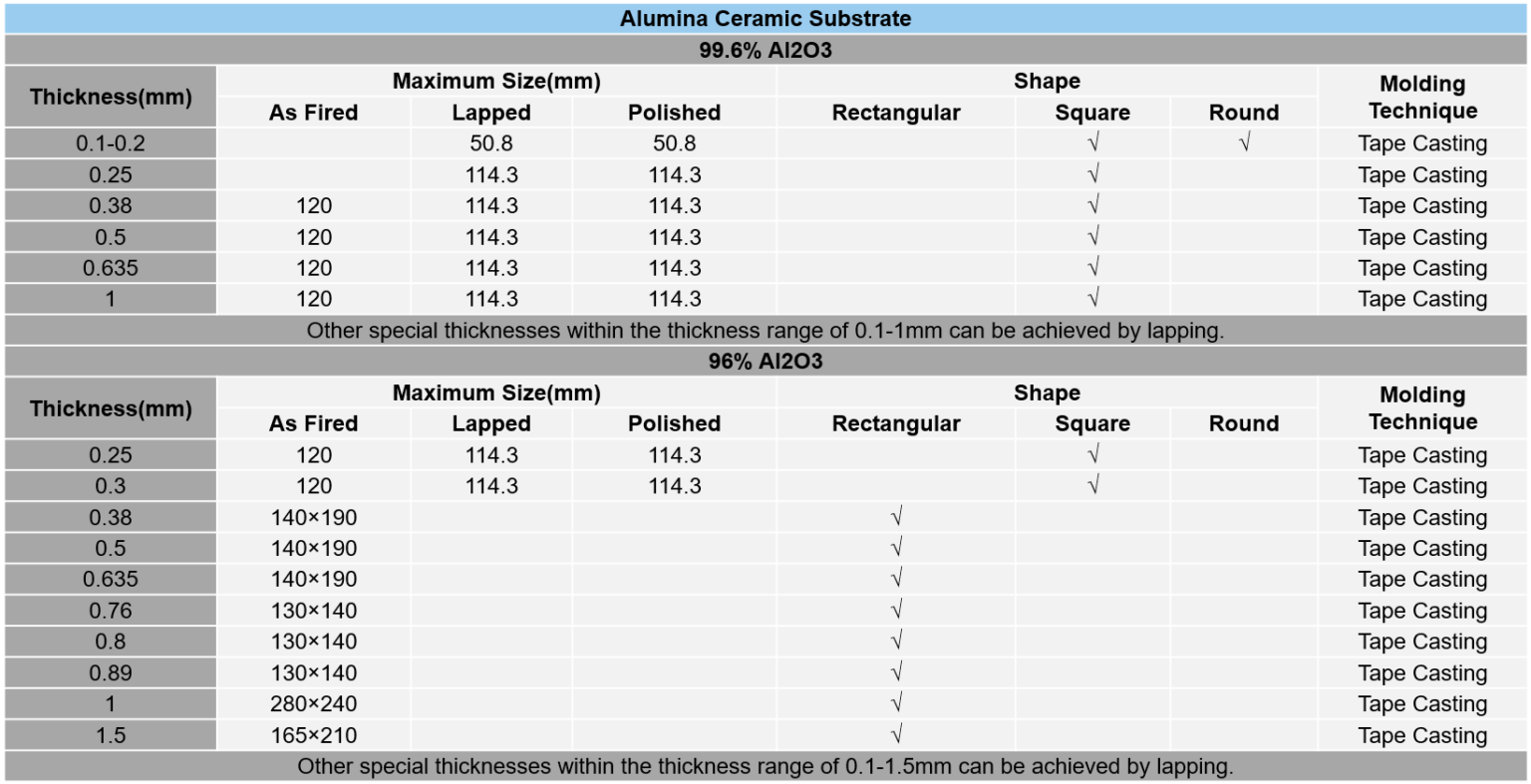
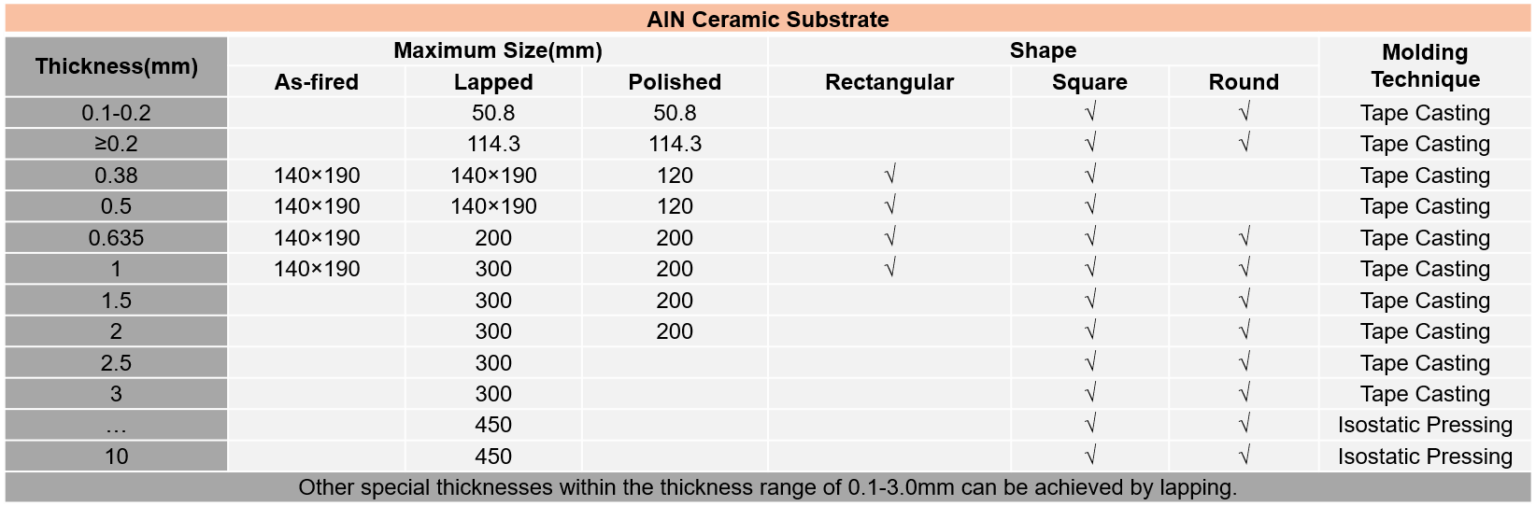
3.4 Standard specifications of our products
We can produce ceramic substrates of various specifications according to customer drawings. The table below shows our standard thicknesses and sizes.
3.4.1 Alumina ceramic substrates
3.4.2 Aluminum nitride ceramic substrates
4. Testing of ceramic substrates
4.1 Appearance inspection
The appearance inspection of ceramic substrates generally uses the naked eye or microscope to detect whether there are cracks and holes on the surface of the substrate, and whether there are quality defects such as bubbles, delamination, scratches or stains on the surface of the metal layer. In addition, the size of the ceramic substrate, substrate flatness (warpage), metal circuit layer thickness and surface roughness, line width and spacing, etc. are all important inspections.
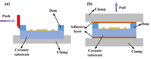
4.2 Common bond strength testing methods
4.2.1 Adhesive tape method
stick 3M adhesive tape to the surface of the metal layer, and roll it with a rubber roller to remove air bubbles in the bonding surface. After 10s, use a pulling force perpendicular to the metal layer to peel off the tape to detect whether the metal layer is peeled off from the substrate, which is a qualitative test method.
4.2.2 Wire welding method
select a metal wire with a diameter of 0.5 mm or 1.0 mm, and directly weld it on the metal layer of the substrate through solder melting, and then measure the tensile force of the metal wire along the vertical direction with a tensile gauge.
4.2.3 Peel strength method
Etch (cut) the metal layer on the surface of the ceramic substrate into 5 mm x 10 mm strips, and then tear it off in the vertical direction on a peel strength testing machine to test its peel strength. The peeling speed is required to be 50mm/min, and the measurement frequency is 10 times/s.
Commonly used test methods include shear strength test and tensile strength test as follows.
4.3 Reliability testing and analysis
Reliability mainly tests the performance changes of ceramic substrates in specific environments (high temperature, low temperature, high humidity, radiation, corrosion, high frequency vibration, etc.). The main contents include heat resistance, high temperature storage, high and low temperature cycle, thermal shock, corrosion resistance , corrosion resistance, high frequency vibration, etc. For failed samples, scanning electron microscope (SEM) and X-ray diffractometer (XRD) can be used for microcosmic and component analysis respectively; scanning acoustic microscope (SAM) and X-ray detector can be used for welding interface and defect analysis.
the Future Trends
The future development trends of ceramic substrates mainly include the following directions.


Why Choose Us
As a manufacturer of ceramic substrates, we have the following advantages:
1. Strict Quality Management System
Each department of the factory strictly implements the ISO9001:2015 quality management system, and passes the ISO14000 environmental management system.
2. Reliable Product Quality
Carefully selected high-quality materials are used to make the substrate, and advanced production technology and testing methods are adopted to ensure the quality of the product and the consistency of each batch.
3. One-stop Production Capacity and Controllable Cost
Strong comprehensive production capacity, self-owned molding, sintering, laser scribing/cutting, metallization production line, can provide customers with professional technical support and optimized solutions.
4. Various Product Specifications
For details, refer to the relevant chapters of “Knowledge”.
5. Good Reputation
Our cooperation cases with many domestic and foreign customers prove that our products and services have been recognized and trusted by customers.
FAQs
The FAQs (Frequently Asked Questions) column is designed to provide users with fast and convenient answering services. We hope that through the FAQs column, we can help you better understand our products and services. If you have any suggestions or comments on the FAQs column, please feel free to contact us.
1.What is the best way to cut ceramic substrates?
It depends a bit on the shape and precision you are trying to achieve. In general, laser cutting is the best way to do it but be aware that laser cutting is very difficult, and conductive residue might be formed at the edges. Alternatives are diamond drills and diamond saws if precision is less a requirement. We have had customers that cut the substrates into shape with a Dremel and a diamond cutting blade. Just make sure you always use cooling or cut small parts at a time.
Last but not least, for straight cuts, you can scribe and cleave the boards using a diamond-tipped scribing pen. It requires a bit of practice but will work well for thinner substrates below 0.635mm (0.030").
2.How are the ceramic substrates machined?
We use 100% laser processes. This is the best way to ensure precise and clean milling and drilling of the ceramic.Laser scribing is one of the laser processing methods. It is drilling a series of blind holes in a line to create a weak spot in the material and ensure a clean cut when breaking out.
3.What sizes are available for the Alumina substrates?
The typical largest size available is 200x160mm. Rectangular shapes are available up to 430x110mm. Maximum standard thickness is 1.27mm and up to 2.0mm thicknesses are available per request. We offer customized products for special requirements.
4.Can you make an Alumina substrate with a 0.1mm thickness?
Unfortunately, 0.1mm thick Alumina substrates are not currently available. These are in the development stage. Please contact for specific requirements.
5. What is the via diameter available for Alumina substrates?
Round vias with diameters of 0.2mm are available. Square holes and special shape holes are also available per request. Please contact us for details.
6.What type of conductor material are available for the thick film circuit substrates?
Silver-Platinum (AgPt), Silver-Palladium (AgPd), Gold (Au) are available for thick film conductors. Ni-Au plating finish is available for Silver-Platinum (AgPt), Silver-Palladium (AgPd). Pb-free conductor material is also available. Please contact for details.