Overview: What is TPC?
Thick Film Printing Ceramic Substrate (TPC) is a manufacturing process that applies metal pastes (e.g., Ag, Cu, or Au-based) onto ceramic surfaces via screen printing, followed by high-temperature sintering (850–900°C) to form circuit patterns. TPC is widely used in automotive electronics, industrial power modules, and LED lighting due to its cost-effectiveness, excellent thermal stability, and design flexibility.
Unlike thin-film ceramics (TFC) that rely on vacuum sputtering and photolithography, TPC employs an additive manufacturing approach, layering circuits through printing, significantly reducing equipment costs and production expenses. However, limited by screen printing resolution, TPC typically achieves line widths ≥100μm, making it suitable for medium-precision applications requiring high voltage/current tolerance.
Core Technical Principles and Process Characteristics
Process Flow
TPC manufacturing involves three key steps: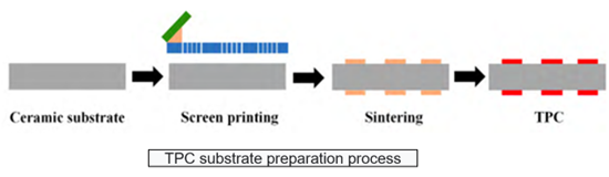
Paste Preparation: Metal powders (Ag, Cu, or Au), glass binders, and organic vehicles are mixed to form printable pastes. Glass phases (5–10%) reduce sintering temperature and enhance ceramic-metal adhesion but slightly compromise conductivity.
Screen Printing: Paste is transferred through stainless steel meshes (80–200 mesh counts) to ceramic substrates (Al₂O₃, AlN, or Si₃N₄). Jinghui Ceramics uses high-precision servo-driven printers (e.g., JY-IC-200A) for ±0.01mm alignment accuracy.
High-Temperature Sintering: Conducted in inert atmospheres (N₂ or Ar) to melt metal particles and form chemical bonds with ceramics. Typical sintering temperatures are 850–900°C for Al₂O₃ and 900–950°C for AlN (requires pre-oxidation).
Performance Advantages
Thermal Management:
Al₂O₃ TPC thermal conductivity: 24–30 W/m·K; AlN TPC: 170–200 W/m·K, ideal for power device cooling.Mechanical Strength:
Ceramic-metal bond strength >15 MPa (ASTM F1841), resistant to thermal cycling (-40°C to 150°C) without delamination.Cost Efficiency:
No vacuum equipment needed, reducing production costs by 30–40% compared to DPC (Direct Plated Copper).
Limitations and Innovations
Traditional TPC faces challenges like limited resolution (line width ≥100μm) and reduced conductivity due to glass phases (copper paste resistivity <5 mΩ·cm). In recent years, the following technologies have achieved breakthroughs in the industry: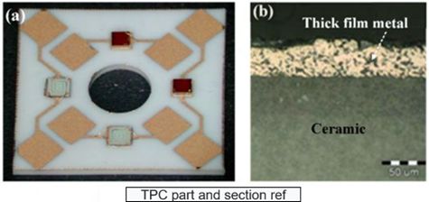
Laser Dry Etching Hybrid Process:
Combines thick-film printing with femtosecond laser etching to achieve 20μm fine lines, increasing wiring density by 300%.Glass-Free Pastes:
Nano metal particles (<1μm) and reactive binders (e.g., TiH₂) form TiN interface layers during sintering, ensuring high conductivity (resistivity <2 mΩ·cm) and strong adhesion (>20 MPa).
Industry Applications of TPC
| Field | Application Examples | Performance Requirements |
|---|---|---|
| Automotive | Engine sensor modules, ECU boards | Resists -40°C–150°C cycling, resistivity <5mΩ·□ |
| Industrial Power | IGBT drivers, solar inverters | Thermal conductivity >20 W/m·K, breakdown voltage >2.5 kV |
| LED Lighting | COB substrates, automotive lighting | Reflectivity >90%, UV resistance |
| Consumer Electronics | Smart appliance PCBs, wireless charging coils | Cost-sensitive, min. line width 150μm |
TPC vs. Alternative Ceramic Substrate Technologies
| Parameter | TPC | DPC | AMB |
|---|---|---|---|
| Min. Line Width | 100μm | 20μm | 200μm |
| Metal Thickness | 10–20μm | 5–15μm | 100–600μm |
| Thermal Cond. (AlN) | 170–200 W/m·K | 200–220 W/m·K | 200–220 W/m·K |
| Production Cost | Low (no vacuum needed) | Medium (complex plating) | High (expensive brazing) |
| Best For | Mid-power, cost-effective | High-precision, high-frequency | High-power, high-reliability |
Future Trends: Innovation Directions for TPC
High-Density Integration:
Laser etching and multi-layer printing enable ≤20μm line widths for SiC/GaN semiconductor integration.Hybrid Process Integration:
Combines TPC with thin-film surface treatments (e.g., sputtered Cu) to improve surface flatness (Ra <0.1μm) and high-frequency performance.Green Manufacturing:
Water-based pastes and lead-free glass binders reduce VOC emissions by 50%, complying with EU RoHS standards.
Frequently Asked Questions (FAQ)
Q1: Can TPC substrates be used for high-frequency (>5GHz) applications?
A1: Traditional TPC is limited to ≤5GHz due to high surface roughness (Ra≈0.5μm) and dielectric loss from glass phases. Jinghui’s polished surfaces + glass-free pastes reduce loss tangent (tanδ) to 0.002, supporting up to 10GHz.
Q2: How to address CTE mismatch between TPC metal layers and ceramics?
A2: Graded metallization (e.g., Cu-Mo-Cu pastes) and stress buffer layers (ZrO₂ particles) transition CTE from ceramic (7×10⁻⁶/K) to copper (17×10⁻⁶/K), reducing thermal stress cracks.
Q3: What is TPC’s reliability in high-temperature/humidity environments?
A3: Cr₂O₃-doped glass frits enhance hydrolysis resistance. Tests show <3% resistance drift and >90% bond strength retention after 500h at 85°C/85% RH.
Q4: Is 3D curved substrate printing supported?
A4: Yes. Flexible screens and adaptive squeegee systems enable printing on curved surfaces (e.g., tubular heat exchangers with radius >5mm) with ±0.05mm accuracy.
Q5: How to balance cost vs. performance between TPC and DPC?
A5: TPC suits mid-volume, cost-driven applications (e.g., automotive sensors), costing 40% less than DPC. DPC is ideal for high-precision/high-frequency needs (e.g., LiDAR) but involves costly plating processes