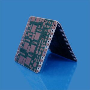
About Alumina Substrate with Copper Metallization
Aluminum oxide substrate with copper metallization is a kind of metallized alumina substrate. Alumina substrate is a material with excellent insulating properties and good thermal conductivity, which is widely used in the fields of electronics, optoelectronics and semiconductors. However, in some applications, electrical conduction on the alumina substrate is required, which requires metallization of the alumina substrate. Alumina substrates with copper metallization usually achieve circuit conduction by depositing a layer of copper metal film on the surface of alumina.
The most commonly used methods for copper metallization on alumina substrates are DPC and DBC.
(1) Direct Plated Copper (DPC) substrate
The production process of DPC substrate is to pre-clean the ceramic substrate, use the semiconductor process to sputter the copper seed layer on the ceramic substrate, and then form the circuit pattern through photolithography processes such as exposure, development, etching, and film removal and finally increase the thickness of the copper circuit by electroplating or electroless plating, and the surface metallization of ceramic substrates is completed after removing the photoresist.

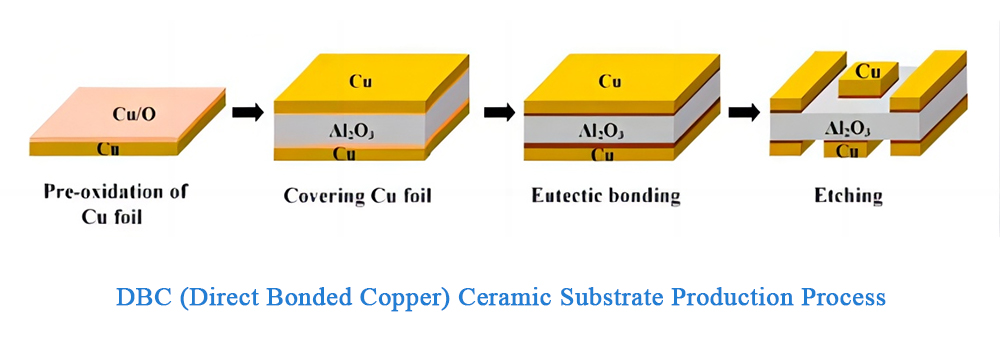
(2) Direct Bonded Copper (DBC) substrate
Oxygen is added between copper and ceramic to obtain a Cu-O eutectic liquid at a temperature of 1065-1083°C, and then react to obtain an intermediate phase (CuAIO2 or CuAI2O4), thereby realizing chemical metallurgy bonding between Cu layer and ceramic substrate. Finally, the photolithography technology is used to realize the pattern and form the circuit.
Characteristics of Alumina Substrate with Copper Metallization
(1) The DPC method is widely used in the LED field. This process has high circuit precision and smooth surface, and is more suitable for flip-chip/eutectic packaging.
(2) The DBC method is often used in high-power modules. The copper layer is thicker, can carry a large current, has good thermal conductivity, high strength, strong insulation, and the thermal expansion coefficient matches semiconductor materials such as Si.
Our Advantages
Jinghui has more than 15 years of experience in the manufacture of metallized ceramic substrates, and can carry out proofing or mass production according to the product drawings and customer requirements. Welcome to inquire.


")
")